Making Composite Prints Space-Ready
The thing with breakthroughs is that they are where the real work starts. Once the capability to print simultaneously with two blends of PEEK had been achieved, the RnD team at Zortrax started perfecting the technology.

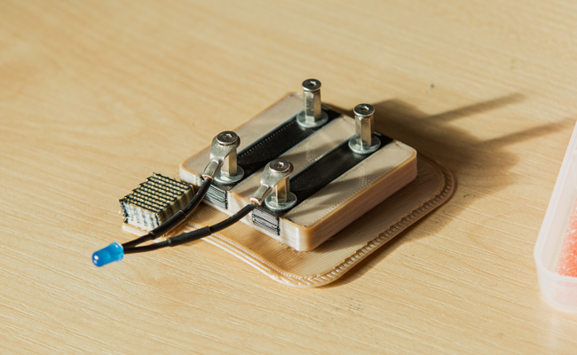
First PEEK-Conductive PEEK composite models printed for the European Space Agency.
Models printed with this technique were impressive but to make them ready for spaceflight several issue had to be . Improvements were made in three key areas.
- Dimensional accuracy had to be improved to enable printing smaller parts that would fit on CubeSats
- Conductivity of the paths made with conductive paths had to be increased to make power and data transferring less energy intensive
- Gaps in the printed models had to be eliminated to get rid of air trapped in the models which could expand under vacuum
It was quite a challange to achieve just a single one of these goals. In under a year, Zortrax managed to reach all of them. Here’s how.
Improving Dimensional Accuracy with PEEK
PEEK is a material extremely difficult to print with. It has very high melting temperatures which means the 3D printer has to support extrusion in over 400°C to start processing it. Then, PEEK contracts significantly when cooling down to room temperature which has to be accounted for. This contraction introduces internal stresses into the printed part which can cause cracking or warping.

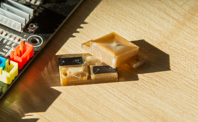
Miniaturized version of the conductive demonstrator printed for the WISA Woodsat mission.
So, first composite prints were relatively large. Talking about a size comparable to a couple of matchboxes which is quite significant considering a standard CubeSat is just 10 cm x 10 cm x 10 cm. Still, in those first proof-of-concept models there were imperfections.
These imperfections were there partially because at the beginning Zortrax engineers used printing temperatures exceeding 430°C which was very high even for PEEK. The reason behind this was to achieve uniform distribution of graphene nano-particles and carbon nanotubes present in the conductive PEEK to increase conductivity of the conductive paths. This goal was achieved at a cost of dimensional accuracy.

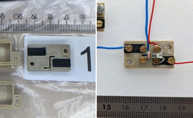
Flight ready demo-circuit with connected cables during integration process at ESA ESTEC facility in Netherlands.
By improving PEEK printing profiles and algorithms working in Z-SUITE software, Zortrax team managed to bring the printing temperatures back to more standard 400 °C for both standard and conductive PEEK blends with no adverse effect on conductivity. Details became more pronounced, edges sharper and surfaces smoother as the PEEK material extruded in lower temperature could be precisely deposited in just the right spots by the printing head. This way, making a composite PEEK demonstrator the size of a small post stamp became a reality.
Increasing Electrical Conductivity in ESA’s PEEK
Even at the early stages of the project, Zortrax engineers managed to exceed conductivity values initially achieved by ESA with conductive PEEK filament. ESA, while developing this material, used now discontinued INDMATEC HPP 155 3D printer for test prints. This machine could not reach the printing temperatures possible to achieve on the Endureal. It also lacked a heated printing chamber which made maintaining a stable high temperate around the part being printed impossible.

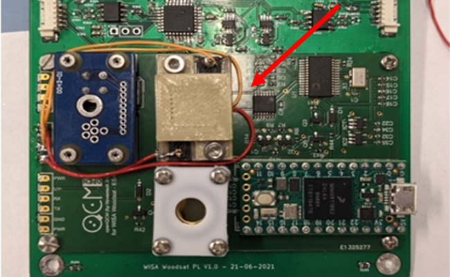
PEEK-Conductive PEEK demonstrator installed on the WISA Woodstat PCB.
The initial improvement in conductivity was possible because the Endureal offered more advanced options for thermal management. But Zortrax team believed more could be done and looked to increase the conductivity even further. This was achieved through modifying software.
Initial tests performed with models 3D printed with ESA’s conductive PEEK showed that the conductivity in the material was anisotropic. It was relatively high, provided the current flew along the paths followed by a printing head when the model was printed. It was disappointingly low, however, when the electrons were forced to flow against those paths. In a typical 3D printed part made with 100% infill with 45-degrees raster angle, the current flew against the paths in almost all scenarios.

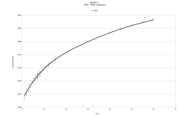
Conductivity in 3D printed paths has reached 0.8 S/m at 30V which is an 8 times improvement made in just 9 months.
To solve this, Zortrax team employed an experimental Z-SUITE feature that radically change the pathing followed by a printing head in the Endureal. Working in this mode, the printer begins printing the object from its outer rim and then proceeds to deposit ever smaller rims moving inward. This technique is used to improve mechanical properties of 3D prints but it also caused an 8 times increase of conductivity values in conductive PEEK models. This bump was possible because in the printed models, electrons could always flow along the paths followed by a printing head.
Eliminating Air Gaps in PEEK 3D Prints
The same printing mode helped deal with air gaps in very small models that appeared between the outer wall of the part and the infill. ESA engineers working on integrating the demonstrator on the WISA CubeSat were concerned that such gaps could contain air which would rapidly expand in vacuum when the printed circuit has reached space.

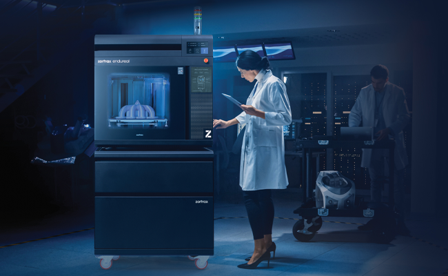
Zortrax Endureal 3D printer used for printing composite parts with two blends of PEEK.
By changing the pathing the Endureal’s printing head used to fabricate the part, such gaps have been practically eliminated. The demonstrator that finally got installed onboard the satellite and passed all demanding tests needed for flight clearance was a near solid structure, a feat that is very difficult to achieve in printing very small objects with high-performance polymers.
Advanced Materials for Space Industry
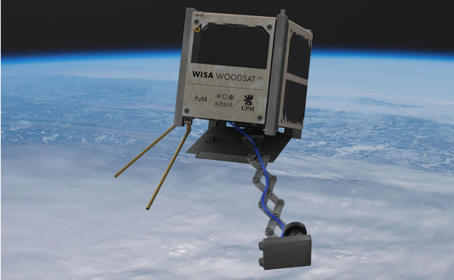
WISA Woodsat is a unique mission focused on testing new materials and groundbreaking manufacturing technologies in space industry. Several parts of this CubeSat are made of birch wood covered with a special kind of coating that is supposed to protect it from space environment effect. It will be launched onboard a partially recoverable Electron rocket which has large parts of its body fabricated with lightweight carbon composites. Obviously, flight-testing 3D printed PEEK electrical circuits for the first time in history fits great in the overall theme of this groundbreaking mission. We believe that innovative materials and additive manufacturing will make space more accessible and easier to reach for businesses and scientists worldwide. And Zortrax has a major role to play in shaping this future.
WISA Woodsat with Zortrax 3D printed demonstrator onboard is scheduled for launch in the first half of 2022 from New Zealand. Apart from printing the PEEK demonstrator with embedded electrically conductive paths, Zortrax is currently working with ESA on two new research projects. Stay tuned and follow Zortrax Official Blog to learn more about them in the future.
The WISA Woodsat has been initiated and is led by Arctic Astronautics, a Finnish company specializing in CubeSat components and developing space technologies for education. Birch wood for the satellite’s frame has been supplied by UPM Plywood, a global manufacturer of plywood and veneer products. A deployable “selfie stick”, which is another 3D printed instrument that will fly on WISA Woodsat mission, has been 3D printed by Delva, a Finnish metal 3D printing company.
*The view expressed herein can in no way be taken to reflect the official opinion of the European Space Agency.
